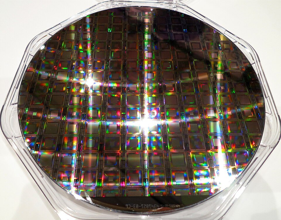
When a chip fabrication plant discovers a pattern of low-yielding wafers, finding the root cause can take weeks. Engineers set up expensive Design of Experiment tests, dedicate operators to track wafers manually, and wait for results. And the test lot may not even reproduce the problem.
A technique called wafer randomization promises to change that, and according to a detailed technical analysis published by Microtronic on June 18, it can dramatically accelerate defect root cause detection without requiring additional equipment or cycle time.
Wafers in a fab move through hundreds of process steps in batches. When a defect emerges, traditional investigation methods involve setting up a new Design of Experiment and a Special Work Request, dedicating engineers and operators to physically randomize wafers and track slot positions, then waiting for results. The whole process takes weeks or months, and success depends on whether the test lot happens to show the same defect.
Without randomization, repeated observations might show five low-yielding wafers consistently appearing in positions 21 through 25 of a cassette. But there is no way to determine which process step caused the problem. The pattern could come from any of hundreds of steps between the start of processing and the inspection point.
How Randomization Works
Wafer randomization is conceptually simple. Instead of keeping wafers in fixed slot positions throughout processing, each batch is shuffled before entering each process step. The slot position of every wafer is precisely tracked.
When a defect pattern emerges after randomization, the data carries positional signatures that point directly to the root cause. A defect affecting every fourth wafer suggests a four-channel processing tool. A pattern clustered in the last five slots of a cassette points to an issue between two specific process steps.
In the Microtronic analysis, randomization narrowed a defect’s probable source from hundreds of process steps to a window between points 130 and 170 of the manufacturing flow, allowing engineers to focus investigation on roughly 40 steps instead of the entire process.
The Microtronic EAGLEview Approach
Microtronic’s EAGLEview is an automated macro wafer defect inspection system that integrates randomization into its workflow. Its SlotTrack feature, part of the ProcessGuard software, automatically randomizes all wafers and precisely tracks every slot position.
The system can be turned on and off as needed. When randomization is active, every wafer automatically becomes a useful test vehicle. There is no need to set up special DOEs, purchase additional sorters, or accept cycle time reduction.
The key advantage is that randomization does not add latency or cost to the manufacturing flow. It uses existing wafer handling and tracking infrastructure, layered with software that correlates slot-position data with yield results.
Why It Matters
As semiconductor manufacturing pushes to smaller nodes and more complex process flows, defect isolation becomes harder and more expensive. At Intel 18A and competing nodes with hundreds of steps, the difference between finding a defect in hours versus weeks translates directly to manufacturing cost and yield improvement.
The technique is not limited to any specific process node or fab. Any facility with automated wafer handling and yield tracking can implement randomization. The cost is primarily in software integration, not hardware.
For the foundry customers that companies like Intel, TSMC, and Samsung are competing to attract, faster defect resolution means faster time-to-market and lower per-wafer costs. In an industry where every percentage point of yield improvement is worth billions, a technique that finds defects in days instead of weeks represents a meaningful competitive advantage.
Sources: Semiconductor Engineering (June 18, 2026)